2025 Stacked Die Microelectronics Packaging Market Report: Growth, Technology Shifts, and Strategic Insights for the Next 5 Years. Explore Key Trends, Forecasts, and Competitive Dynamics Shaping the Industry.
- Executive Summary & Market Overview
- Key Technology Trends in Stacked Die Microelectronics Packaging
- Competitive Landscape and Leading Players
- Market Growth Forecasts (2025–2030): CAGR, Revenue, and Volume Analysis
- Regional Market Analysis: North America, Europe, Asia-Pacific, and Rest of World
- Future Outlook: Emerging Applications and Investment Hotspots
- Challenges, Risks, and Strategic Opportunities
- Sources & References
Executive Summary & Market Overview
Stacked die microelectronics packaging refers to the integration of multiple semiconductor dies within a single package, arranged vertically to optimize space, performance, and functionality. This advanced packaging technology is pivotal in meeting the escalating demands for miniaturization, higher performance, and energy efficiency in sectors such as consumer electronics, automotive, telecommunications, and data centers. As of 2025, the global market for stacked die microelectronics packaging is experiencing robust growth, driven by the proliferation of 5G devices, artificial intelligence (AI) applications, and the Internet of Things (IoT).
According to Gartner, the stacked die packaging market is projected to achieve a compound annual growth rate (CAGR) of over 8% between 2023 and 2027, with revenues expected to surpass $12 billion by 2025. This growth is underpinned by the increasing adoption of 3D integrated circuits (3D ICs), system-in-package (SiP) solutions, and high bandwidth memory (HBM) modules, all of which leverage stacked die architectures to deliver enhanced performance and reduced form factors.
Key industry players such as TSMC, Samsung Electronics, and Intel Corporation are investing heavily in research and development to advance through-silicon via (TSV) and wafer-level packaging (WLP) technologies. These innovations are enabling higher interconnect densities, improved thermal management, and lower power consumption, which are critical for next-generation applications in AI accelerators, advanced driver-assistance systems (ADAS), and high-performance computing (HPC).
Regionally, Asia-Pacific dominates the stacked die packaging market, accounting for more than 60% of global production capacity, largely due to the presence of leading foundries and OSAT (outsourced semiconductor assembly and test) providers in countries such as Taiwan, South Korea, and China. North America and Europe are also witnessing increased adoption, particularly in automotive electronics and data center infrastructure, as noted by IC Insights.
In summary, stacked die microelectronics packaging is a cornerstone technology for the semiconductor industry’s evolution in 2025, enabling higher integration, performance, and efficiency across a broad spectrum of applications. The market’s trajectory is shaped by ongoing technological advancements, strategic investments by leading players, and the relentless demand for smarter, smaller, and more powerful electronic systems.
Key Technology Trends in Stacked Die Microelectronics Packaging
Stacked die microelectronics packaging is at the forefront of semiconductor innovation, enabling higher device performance, increased functionality, and reduced form factors by vertically integrating multiple semiconductor dies within a single package. As the industry moves into 2025, several key technology trends are shaping the evolution and adoption of stacked die packaging solutions.
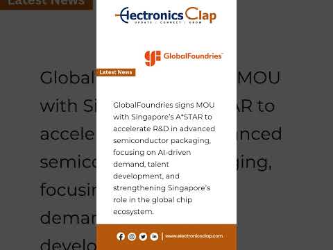
- Advanced Through-Silicon Via (TSV) Integration: TSV technology remains a cornerstone for high-density die stacking, offering low-latency, high-bandwidth interconnects between vertically aligned dies. In 2025, manufacturers are refining TSV processes to reduce via diameter and pitch, thereby increasing interconnect density and improving electrical performance. This is particularly critical for high-performance computing (HPC) and artificial intelligence (AI) applications, where memory bandwidth is a bottleneck. TSMC and Samsung Electronics are leading the charge in commercializing advanced TSV-based 2.5D and 3D IC packaging.
- Hybrid Bonding Techniques: Hybrid bonding, which combines direct copper-to-copper and dielectric-to-dielectric bonding, is gaining traction as a method to achieve ultra-fine pitch interconnects and improved electrical characteristics. This technology is enabling sub-10-micron pitch stacking, which is essential for next-generation logic-memory integration. Amkor Technology and Intel Corporation have announced significant investments in hybrid bonding for both memory and logic devices.
- Heterogeneous Integration: The trend toward integrating diverse chiplets—such as logic, memory, RF, and analog—within a single stacked package is accelerating. This approach allows for optimized process nodes for each function, improving overall system performance and power efficiency. The SEMI industry association highlights heterogeneous integration as a key enabler for advanced automotive, 5G, and edge computing solutions.
- Thermal Management Innovations: As die stacking increases power density, advanced thermal interface materials (TIMs), microfluidic cooling, and integrated heat spreaders are being developed to manage heat dissipation. Yole Group reports that effective thermal management is now a primary differentiator in stacked die package design, especially for data center and AI accelerator markets.
- Automated Test and Inspection: The complexity of stacked die assemblies necessitates advanced test and inspection solutions, including high-resolution X-ray and AI-driven defect detection. KLA Corporation and Teradyne are expanding their offerings to address the unique challenges of multi-die package reliability and yield.
These technology trends are collectively driving the stacked die microelectronics packaging market toward greater integration, performance, and reliability, positioning it as a critical enabler for next-generation electronic systems in 2025 and beyond.
Competitive Landscape and Leading Players
The competitive landscape of the stacked die microelectronics packaging market in 2025 is characterized by intense innovation, strategic partnerships, and a focus on advanced manufacturing capabilities. This sector is driven by the demand for higher device performance, miniaturization, and integration in applications such as smartphones, high-performance computing, automotive electronics, and IoT devices. Key players are leveraging their expertise in wafer-level packaging, through-silicon via (TSV) technology, and heterogeneous integration to maintain a competitive edge.
Leading the market are established semiconductor packaging and assembly service providers, including Amkor Technology, ASE Technology Holding, and TSMC. These companies have made significant investments in R&D and production capacity to support high-volume manufacturing of stacked die solutions. For instance, TSMC’s advanced CoWoS (Chip-on-Wafer-on-Substrate) and SoIC (System on Integrated Chips) technologies are widely adopted for high-end computing and AI applications, while Amkor Technology and ASE Technology Holding offer a broad portfolio of 2.5D and 3D packaging services for consumer and enterprise markets.
IDMs (Integrated Device Manufacturers) such as Intel Corporation and Samsung Electronics are also prominent, integrating stacked die packaging into their product roadmaps to enhance chip performance and power efficiency. Intel’s Foveros technology and Samsung’s X-Cube platform exemplify proprietary approaches to vertical integration and chiplet-based architectures.
Emerging players and niche specialists, including JCET Group and Powertech Technology Inc., are gaining traction by offering customized solutions and targeting specific verticals such as automotive and industrial electronics. These companies often collaborate with fabless semiconductor firms and system integrators to deliver tailored stacked die packages.
The competitive environment is further shaped by ongoing M&A activity, technology licensing, and joint ventures, as companies seek to expand their capabilities and global reach. According to Yole Group, the market is expected to see continued consolidation, with leading players investing in next-generation interconnects, advanced materials, and automation to address the evolving needs of AI, 5G, and edge computing markets.
Market Growth Forecasts (2025–2030): CAGR, Revenue, and Volume Analysis
The stacked die microelectronics packaging market is poised for robust growth between 2025 and 2030, driven by escalating demand for high-performance, miniaturized electronic devices across consumer electronics, automotive, and data center applications. According to projections by MarketsandMarkets, the global 3D IC and stacked die packaging market is expected to register a compound annual growth rate (CAGR) of approximately 12% during this period. This growth trajectory is underpinned by the increasing adoption of advanced packaging solutions to address the limitations of traditional 2D architectures, particularly in terms of power efficiency, form factor, and bandwidth.
Revenue forecasts indicate that the stacked die microelectronics packaging segment will surpass USD 15 billion by 2030, up from an estimated USD 8.5 billion in 2025. This surge is attributed to the proliferation of artificial intelligence (AI), 5G infrastructure, and edge computing, all of which require higher interconnect density and improved thermal management—key advantages offered by stacked die architectures. Gartner highlights that the semiconductor industry’s shift toward heterogeneous integration and system-in-package (SiP) solutions will further accelerate the adoption of stacked die packaging technologies.
In terms of volume, the number of stacked die units shipped is projected to grow at a CAGR of 13–14% from 2025 to 2030, reflecting both increased penetration in high-volume consumer devices and expanding use in automotive electronics and industrial IoT. Yole Group reports that leading foundries and OSATs (Outsourced Semiconductor Assembly and Test providers) are ramping up investments in advanced packaging lines to meet this anticipated demand, with Asia-Pacific remaining the dominant production hub due to its established semiconductor manufacturing ecosystem.
- CAGR (2025–2030): 12–14%
- Revenue (2030): USD 15+ billion
- Volume Growth: Driven by consumer electronics, automotive, and data center applications
- Key Regions: Asia-Pacific leads, followed by North America and Europe
Overall, the stacked die microelectronics packaging market is set for significant expansion, propelled by technological innovation and the relentless push for higher performance and integration in next-generation electronic systems.
Regional Market Analysis: North America, Europe, Asia-Pacific, and Rest of World
The global market for stacked die microelectronics packaging is experiencing dynamic growth, with regional trends shaped by technological innovation, end-user demand, and supply chain developments. In 2025, North America, Europe, Asia-Pacific, and the Rest of World (RoW) regions each present distinct market characteristics and growth drivers.
- North America: The North American market is propelled by robust investments in advanced semiconductor manufacturing and a strong presence of leading technology firms. The region benefits from significant R&D activities, particularly in the United States, where the push for domestic chip production is supported by government initiatives such as the CHIPS Act. Key applications include high-performance computing, automotive electronics, and defense systems. According to Semiconductor Industry Association, North America is expected to maintain steady growth in stacked die packaging, driven by demand for miniaturized, high-density solutions in AI and 5G infrastructure.
- Europe: Europe’s market is characterized by a focus on automotive, industrial automation, and IoT applications. The region’s emphasis on quality and reliability, along with stringent regulatory standards, fosters adoption of advanced packaging technologies. Initiatives such as the European Chips Act aim to bolster local semiconductor capabilities. According to SEMI, European manufacturers are increasingly investing in stacked die solutions to support the region’s growing electric vehicle and smart manufacturing sectors.
- Asia-Pacific: Asia-Pacific dominates the global stacked die microelectronics packaging market, accounting for the largest share in 2025. This leadership is underpinned by the presence of major foundries and OSAT (Outsourced Semiconductor Assembly and Test) providers in countries like Taiwan, South Korea, China, and Japan. The region’s rapid adoption of consumer electronics, smartphones, and data centers fuels demand for high-density packaging. According to IC Insights, Asia-Pacific’s market growth is further accelerated by government incentives and aggressive capacity expansions by leading players.
- Rest of World (RoW): The RoW segment, including Latin America, the Middle East, and Africa, remains nascent but shows potential for growth as digital transformation initiatives expand. Investments in telecommunications infrastructure and emerging electronics manufacturing hubs are expected to gradually increase demand for stacked die packaging solutions, as noted by Gartner.
Overall, regional dynamics in 2025 reflect a convergence of innovation, policy support, and end-market demand, with Asia-Pacific leading in volume and North America and Europe focusing on high-value, specialized applications.
Future Outlook: Emerging Applications and Investment Hotspots
The future outlook for stacked die microelectronics packaging in 2025 is shaped by rapid advancements in semiconductor integration, the proliferation of AI and high-performance computing, and the growing demand for miniaturized, high-density electronic systems. Stacked die packaging, which involves vertically integrating multiple semiconductor dies within a single package, is increasingly recognized as a key enabler for next-generation devices across several high-growth sectors.
Emerging applications are particularly prominent in data centers, 5G infrastructure, and edge computing. The need for higher bandwidth and lower latency in these environments is driving adoption of 2.5D and 3D stacked die architectures, which offer improved electrical performance and reduced interconnect lengths. In 2025, the integration of high-bandwidth memory (HBM) with logic dies is expected to accelerate, supporting the computational demands of AI accelerators and advanced graphics processors. Companies such as Samsung Electronics and TSMC are investing heavily in advanced packaging lines to meet this demand.
Another emerging application is in the automotive sector, where stacked die packaging is enabling the development of compact, high-reliability modules for advanced driver-assistance systems (ADAS) and autonomous vehicles. The automotive industry’s stringent requirements for thermal management and reliability are pushing innovation in through-silicon via (TSV) and wafer-level packaging technologies, with suppliers like Infineon Technologies and NXP Semiconductors expanding their portfolios to address these needs.
Investment hotspots in 2025 are expected to center around Asia-Pacific, particularly Taiwan, South Korea, and China, where government incentives and robust foundry ecosystems are accelerating R&D and capacity expansion. According to Gartner, the global advanced packaging market is projected to grow at a CAGR of over 7% through 2025, with stacked die solutions representing a significant share of this growth. Venture capital and strategic investments are also flowing into startups developing novel interconnect materials and heterogeneous integration techniques, as highlighted by recent funding rounds tracked by CB Insights.
- AI and HPC: Stacked die packaging for AI accelerators and GPUs
- Automotive: High-reliability, compact modules for ADAS and EVs
- 5G/Edge: Low-latency, high-bandwidth solutions for network infrastructure
- Asia-Pacific: Leading region for investment and manufacturing expansion
In summary, 2025 will see stacked die microelectronics packaging at the forefront of semiconductor innovation, with strong momentum in AI, automotive, and communications, and significant investment activity in Asia-Pacific and advanced materials startups.
Challenges, Risks, and Strategic Opportunities
Stacked die microelectronics packaging, a cornerstone of advanced semiconductor integration, faces a complex landscape of challenges and risks in 2025, but also presents significant strategic opportunities for industry players. The primary technical challenge remains thermal management. As more dies are vertically integrated, heat dissipation becomes increasingly problematic, risking device reliability and performance degradation. Advanced thermal interface materials and innovative heat spreader designs are being explored, but their integration adds cost and complexity to the manufacturing process (SEMI).
Yield and reliability risks are also heightened in stacked die architectures. The increased number of interconnects, such as through-silicon vias (TSVs), raises the probability of defects, impacting overall yield. Furthermore, heterogeneous integration—combining dies from different process nodes or foundries—introduces compatibility and testing challenges. The need for advanced inspection and metrology tools is growing, but these solutions can significantly increase capital expenditure (TechInsights).
Supply chain complexity is another critical risk. Stacked die packaging often requires collaboration across multiple suppliers for wafers, substrates, and assembly services. Disruptions in any segment can delay production and increase costs. Geopolitical tensions and export controls, particularly in the US-China technology trade, further exacerbate supply chain vulnerabilities (Gartner).
Despite these challenges, strategic opportunities abound. The demand for high-performance computing, AI accelerators, and advanced mobile devices is driving rapid adoption of stacked die solutions. Companies that invest in proprietary thermal management, advanced testing, and robust supply chain strategies can differentiate themselves and capture premium market segments. Additionally, partnerships between foundries, OSATs (Outsourced Semiconductor Assembly and Test), and EDA (Electronic Design Automation) vendors are enabling new design and manufacturing paradigms, such as chiplet-based architectures, which can further unlock value (TSMC).
- Thermal management and reliability remain top technical hurdles.
- Yield loss and inspection costs are rising with increased integration complexity.
- Supply chain risks are amplified by geopolitical and logistical factors.
- Strategic investments in R&D, partnerships, and supply chain resilience offer competitive advantages.
Sources & References
- IC Insights
- Amkor Technology
- KLA Corporation
- ASE Technology Holding
- JCET Group
- Powertech Technology Inc.
- MarketsandMarkets
- Semiconductor Industry Association
- Infineon Technologies
- NXP Semiconductors
- TechInsights